April 2025
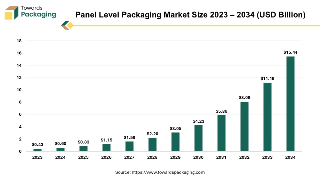
The panel level packaging market is forecast to grow from USD 0.83 billion in 2025 to USD 15.44 billion by 2034, driven by a CAGR of 38.60% from 2025 to 2034.

The panel level packaging market is expected to experience significant growth throughout the forecast period. The panel level packaging market is likely to witness strong growth over the forecast period. Packaging at the panel level is when a package is processed on a square or rectangular surface. As part of the assembly process, panel-level molding, bumping, die attach and redistribution line fabrication are all done. It covers the next generation of fine feature substrates, which need the modern instruments and materials to fabricate structural features (lines, microvias) and it makes use of a variety of manufacturing infrastructures like the Si (BEOL), a printed circuit board, LCD, and photovoltaics. It exceeds the capabilities of established PCB/laminate infrastructure.
The goal of utilizing different infrastructures is to provide high-quality features at an affordable price for particular applications. The increasing demand for miniaturized electronic devices such as the smartphones, wearables and IoT devices are expected to augment the growth of the panel level packaging market during the forecast period. Furthermore, the advancements in AI, 5G and automotive technologies as well as the trend toward heterogeneous integration, where different types of chips are combined into a single package is also anticipated to augment the growth of the market across the globe.
Additionally, the ongoing shift toward smaller, more powerful consumer electronics as well as the rising adoption of PLP in the automotive sector, particularly for the advanced driver-assistance systems (ADAS) and electric vehicles is also projected to contribute to the growth of the market in the years to come.
The demand for miniaturization in the electronics industry is projected to support the growth of the market during the forecast period. For most of the technological advancements, miniaturization has been extremely important. Electronic packaging is one of the many procedures related to semiconductor devices and circuit technology, which acts as the foundation for highly effective, compact electronic systems. Larger batteries can be included into devices without increasing their total size due to the miniaturization of electronic subdivisions, which makes them appealing to end users across nearly all industries.
From a design point of view, smaller modules allow designers more creative freedom to create popular products. From the perspective of technology, smaller modules imply a shorter signal path with less stray capacitance and inductance, which means that signal integrity in increased and high operational speed, would be reliably achieved. For instance, KalamSathas, the tiniest satellite, was launched with success. Being lighter than a smartphone, it is the lightest and most compact satellite in the world.
Moreover, the continuous miniaturization and operational heterogeneity of electronics packaging are driving the demand for improved substrate technologies. Advanced multi-chip packaging systems that are highly integrated connect memory or power management components with application, logic and computational dies in a single package. Close embedding of the thin dies on the IC substrates based on big formats, a technique familiar from PCB manufacturing with panel level packaging (PLP), is one way to reduce the fabrication costs. PLP maximizes material consumption and enables the integration of more complicated circuitry in a smaller footprint by processing multiple chips at once on a bigger panel.
Supporting the sophisticated features that modern devices require such as the fast processing, improved networking and precise sensors is essential. With enormous potential for downsizing and heterogeneous integration, these technology approaches provide several advantages and opportunities for developing the high-performance systems. It is anticipated that the PLP approach will be compliant to the accepted practices in LCD and PCB production, expediting development and commercialization objectives.
The lithography challenges are likely to impede the growth of the panel level packaging market during the forecast period. The lithography problem for large heterogeneous integration originates from the fact that the majority of the presently accessible lithography systems have an exposure field that is limited in size, usually measuring 60mm x 60mm or less. Large substrates can be patterned using smaller-field systems by piecing together several exposures, but this reduces the yield as well as the productivity due to the requirement for multiple exposures of different reticles and the possibility of failures at the stitching limits. Lithography equipment developed for smaller wafers struggle to achieve the same level of precision and detail when used on the panels that can be several hundred millimeters in size. The requirement for fine-line patterning in modern semiconductor applications, where even small deviations might have an impact on performance, makes this problem considerably more difficult.
However, there are drawbacks with a vast exposure surface. These include warpage and distortion of panels, which might affect overlay, crucial dimensions, and uniformity. Warpage is a major problem associated with novel single-die and multi-die packages. Due to misalignment and handling challenges, warpage poses a serious threat to processes like wafer singulation, ball placement and RDL. Furthermore, significant warpage will deteriorate dependability and perhaps cause catastrophic errors like breaking and delamination. This warpage is particularly challenging for the large-scale wafer-level and panel-level processes. As a result, warpage and distortion pose a serious barrier to the panel level packaging market, making it more difficult to implement this technology and requiring advanced techniques to reduce the associated risks.
The growth and investments in semiconductor industry is expected to create immense growth opportunities for the panel level packaging market in the years to come. As global demand for advanced electronic devices continues to surge, fueled by the proliferation of technologies such as 5G, artificial intelligence (AI), autonomous vehicles, and the Internet of Things (IoT), the semiconductor industry is experiencing unprecedented expansion.
In July 2024, the Semiconductor Industry Association (SIA) announced global semiconductor industry sales hit $49.1 billion during the month of May 2024, an increase of 19.3% compared to the May 2023 total of $41.2 billion and an increase of 4.1% compared to the April 2024 total of $47.2 billion. The global semiconductor market has grown on a year-to-year basis during each month of 2024, and year-to-year sales in May increased by the largest percentage since April 2022. The Americas market experienced particularly strong growth, with a year-to-year sales increase of 43.6%.
Furthermore, governments as well as the companies are ramping up their investments in research, development, and production capacities to meet the growing need for more powerful and efficient semiconductor devices. In May 2024, China announced the largest-ever semiconductor investment fund to propel development of the domestic chip industry, the latest effort from Beijing to achieve self-sufficiency as the US seeks to restrict its growth.
The third phase of National Integrated Circuit Industry Investment Fund has amassed 344 billion Yuan ($47.5 billion) from the central government and various state-owned banks and enterprises including Industrial & Commercial Bank of China Ltd. This surge in investment is particularly beneficial for PLP, as it aligns with the industry's pursuit of innovative packaging solutions that can enhance device performance while reducing size and cost. With the semiconductor industry channeling billions of dollars into new manufacturing facilities, equipment, and technology development, there is a significant opportunity for PLP to be adopted on a larger scale.

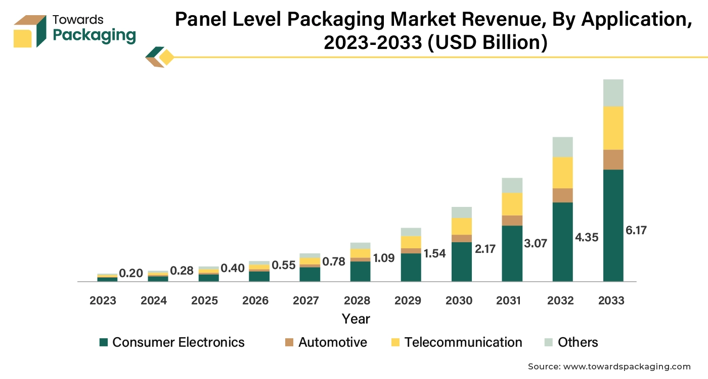
The consumer electronics segment captured largest market share of 47.24% in 2023. This is owing to the ongoing trend towards digitalization and the integration of the smart technologies into everyday life along with the growing demand for a wide range of electronic devices such as the smartphones, tablets, smartwatches and home automation systems. Furthermore, the rise of remote work and online education as well as the deployment of the 5G networks is also likely to support the growth of the segment in the global panel level packaging market during the forecast period. Additionally, the increasing consumer preference for high-performance and multifunctional devices is expected to contribute to the growth of the segment in the years to come.

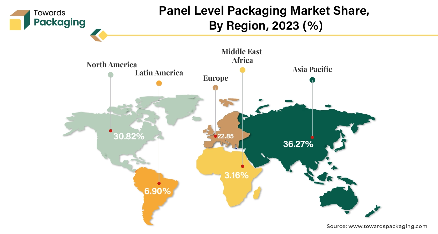
Asia Pacific is likely to grow at fastest CAGR of 40.89% during the forecast period. This is owing to the well-established infrastructure of the semiconductor fabrication as well as the presence of the advanced electronics manufacturing hubs in the economies like China, South Korea, Taiwan and Japan. Furthermore, the growing investment in the semiconductor production is also expected to contribute to the growth of the market in the region.
North America held considerable market share of 30.82% in 2023. This is due to the presence of leading semiconductor companies and research institutions such as Intel Corporation, Qualcomm Incorporated, NVIDIA Corporation and Texas Instruments, among others. Also, the increasing demand for high-performance computing (HPC), driven by the rise of data centers, artificial intelligence (AI) and machine learning applications is further expected to support regional growth of the market in the years to come. Furthermore, the deployment of 5G networks across the region and rise of electric vehicles (EVs) and autonomous vehicles is also expected to support the regional growth of the market in the near future.
By Industry Application
By Region
April 2025
April 2025
April 2025
April 2025