April 2025
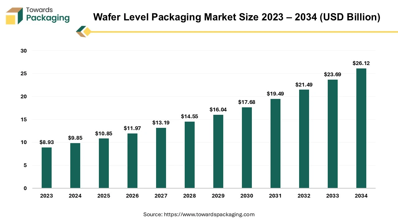
The wafer level packaging market size was calculated at USD 9.85 billion in 2024 and is projected to reach around USD 26.12 billion by 2034. The market is expanding at a CAGR of 10.25% between 2025 and 2034.

Unlock Infinite Advantages: Subscribe to Annual Membership
The growing demand for electronic devices and rapid advancement in the integrated circuits used in mobile devices and the semiconductor market influence the demand for wafer level packaging market. The growing trend for compact electronic devices in several sectors such as automotive, healthcare, and many others driven the growth of wafer level packaging market.
Wafer level packaging (WLP) is the procedure where components are connected to an integrated circuit (IC) before the wafer is diced. In this rising economy there is high demand for mobile and compact electronic devices. There is a huge demand for small-size devices which can be easily carried anywhere in the healthcare sector and can only be possible with wafer level packaging solutions. This type of packaging promotes the miniaturization of electronic parts with enhanced functionality and performance.
The growing demand for wearable watches or fitness bands is a suitable example of miniature electronic devices in the healthcare sector. The rising adaptation of the Internet of Things (IoT) in various sectors amplifies the demand for these packaging. Major market players are contributing significantly to the growth of this market by introducing innovative technology. The introduction of wireless communication devices, sensors, and other such devices growing the demand for wafer level packaging market.
Rapid advancement in semiconductors industry:
The ongoing advancements in semiconductor sector is seen to promote the manufacturing as well as packaging services, especially in Asian countries with massive investments in the semiconductor sector.
Wide use of semiconductors integrated circuits in IoT devices:
As the IoT industry expands, the requirement for wafer is seen to boost in the upcoming years. The demand for wireless devices, cellular devices, and Wi-Fi devices is observed to promote wafer manufacturing.
Rapid expansion of miniature electronic devices:
Wafer packaging for miniature or smaller devices allows chips to continue to reduce in size, which makes it easier to test chip’s functionality.
AI has a significant role in the wafer level packaging market by adding advancement in the manufacturing of semiconductors. It helps in various steps of wafer level packaging such as inspection, designing, testing, and optimization. With the incorporation of AI, the behaviour of the integrated circuit can be identified which is then utilized to produce high quality precise and efficient packaging. In the healthcare sector, AI can detect huge numbers of data from optical scans or X-rays of wafers to identify defects in the human body.
This improves yield and decreases waste, which is important in such a market that is manufacturing high-cost products. Artificial intelligence and machine learning eradicate manual faults in date labelling, product information, consumer details, and many things in between. More significantly, it can safeguard obedience to supervisory necessities while improving brand identity with label plans that sink the competition.
The regular advancement in semiconductor technology fuels the extension of the wafer level packaging market. It is the growing use of semiconductor integrated circuits in the Internet of Things (IoT). The integration of various networks such as 3G, 4G and 5G enhance the telecommunication standards, government guidelines to arrange energy-effective systems and solutions, and developments in wired and wireless communication devices are the major aspects driving the need for these Internet of Things devices.
IoT chipset mandate will upsurge as more IoT techniques are advanced and added to IoT equipment. These IoT applications use chipsets that integrate FOWLP, RF units (MCU), sensor modules, and Wi-Fi. Another important trend driving the growth of the global wafer level packaging market is the upsurge in panel-level packing. The semiconductor corporation has experienced numerous growths as a consequence of the growing demand for high-performance and low-cost goods.
OSAT industries, fabless businesses, IDMs, and substrate makers all use such technology since it severely lowers their industrial charges. The growing demand for electronics in numerous businesses also makes panel-level packing a need for dealers to attain high-volume manufacturing. Therefore, influences the wafer level packaging market profits.
Development of the worldwide wafer level packaging market is expected to be influenced by aspects such as growth in acceptance of compact size, high-speed, and less expensive electronic devices. Moreover, wafer level packaging technique dominance over traditional packaging technology and the approaching requirement of circuit miniaturization in microelectronic equipment influence the market development. The increase in the usage of wafers in the automotive market is anticipated to boost market development during the predicted period.
Major market players are capitalizing profoundly on study and development to enlarge their product appearances, which will aid the wafer level packaging market, and raise even more. Market applicants are also undertaking several planned activities to enlarge their mark, with significant market expansions comprising new product promotions, contractual agreements, collaboration and achievements, higher investments, and association with other establishments.
To enlarge and endure in a more competitive and expanding market, wafer level packaging businesses must offer cost-operative products. Producing locally to reduce the functioning charges is one of the major business strategies used by producers in the wafer level packaging sector to help clients and upsurge the market. In upcoming years, the wafer level packaging sector has presented some of the most important advantages to the healthcare industry.
However, intricacies in the production procedure act as the key limitation for the market. As the intricacy of integrated circuits rises, so do the challenges of testing and confirming their dependability at the wafer level. Additionally, the move in the direction of finer nodes and deeper incorporation means that the WLP technique must endure progress, pushing the limitations of current material and development abilities.
The 3D TSV wafer level packaging segment is leading in the wafer level packaging market and is observed to sustain as a considerable shareholder during the predicted period. In 3D TSV wafer level packaging is used extensively due to its improved capacity, reduced system space supplies, enhanced performance, and less power consumption. In the upcoming years, this aspect would subsidize this segment of the market which is widely expanding rapidly.
Fan-in Wafer Level Packaging (FI-WLP) is leading the material segment of the wafer level packaging market in the predicted period due to the rising demand for compact packaging. The fan in wafer level packaging group produced the most earnings. Fan-in WLP technology dominant in the semiconductor sector, which delivers undeniable benefits in terms of shape and charge is accredited with the continued development of the segment. Moreover, the variability of fan-in-wafer-level packaging arrangements keeps rising due to developments in technology and invention.
In the wafer level packaging market, the consumer electronics segment is highly preferred in the predicted period. Consumer electronics is an extensive segment in the wafer level packaging market, having a high-value share of the market. The expansion of electronic packaging technology has resulted in the creation of enormously operative and consistent electrical connecting approaches for electronic devices, contributing to the stable development of this segment. The consumer electronics group produced the most earnings. The growth of electronic packaging skills, which has resulted in the creation of enormously effective and dependable electrical connecting approaches for electronic devices, is answerable for the steady expansion of the segment.
Asia Pacific witnessed the highest revenue share for the year 2024. It is due to the manufacturing of miniaturized and advanced technology leading the semiconductor businesses and unconventional technological infrastructure that contributes to its leading position. Strong request for cutting-edge consumer electronics and high-presentation computing equipment. Substantial funds in R&D by main semiconductor companies. Favourable government guidelines backup technological progressions. Because of the demand for high-performing, energy-efficient, and small-form factor packages, wafer level packaging is progressively being used in miniature equipment such as smartphones.
Moreover, the country is home to several top producers of electronic packaging, which is helping the market grow. The Asia Pacific region is mainly witnessing constant progressions in packaging techniques, such as fan-out wafer-level packaging and 3D wafer-level packaging are influencing market development across the region. The growing demand for high-performance and miniaturized electronic equipment is driving the acceptance of wafer-level packaging resolutions. Noteworthy investments in study and development by chief semiconductor industries are important to inventions and cost-effective packing solutions.
Europe is estimated to grow at the fastest rate over the forecast period. The development may be a consequence of the noteworthy growth of the manufacturer's savings in the huge production of multifaceted semiconductor equipment. Moreover, initiatives are utilizing wafer-level packaging technology to manufacture products for the aerospace and automotive market, which will suggestively raise market development. Additionally, the German WLP market apprehended a rapidly growing market share, and the UK wafer-level packaging market was the continuously rising market in the European region.

By Type Outlook
By Technology Outlook
By End Use
By Region
April 2025
April 2025
April 2025
April 2025